


Electronic components are getting smaller and smaller. Several inter-related factors explain this trend. The pressure is on end-product manufacturers to make their products smaller yet increase their capabilities and functionality. To achieve that, component manufacturers need to keep innovating their technologies to fit into a smaller space. Technology research and development makes this possible; an excellent example is how semiconductors continue to pack in billions of transistors into an ever-decreasing footprint. But semiconductors are not the only electronic component that needs to get smaller. Today, most electronics-based end-products may only contain less than five semiconductors, even though their capabilities have hugely increased. However, supporting and equally essential components, such as passives (inductors, capacitors, and resistors), are required in the hundreds.
However, component miniaturisation requirements are not limited to just electronic components. Factory floor space is at a premium in the industrial domain, and the space available for each production asset, sensor and actuator are limited. Consequently, the next generation of each production asset needs to be smaller and provide more functionality.
This article focuses on how continued component miniaturisation is paramount in the industrial domain, whether an electronic component or an industrial sensor.
Component miniaturisation strives forward
Change is constant in the electronics industry. Since the birth of the transistor in the late 1940s, researchers embarked on an evolutionary journey that would focus on miniaturisation. A decade later, the first integrated circuit (IC) containing four transistors was developed by Robert Noyce at Fairchild Semiconductor. Fast forward to today, and you’ll find tens of billions of transistors in leading-edge processors. The process of fabricating semiconductors in an increasingly smaller area has advanced significantly. However, the advancements in component design and manufacture have also benefitted the broader electronics industry.
The impact of technology advancements for electronic components
The first transistor prototype was a large item compared to today’s devices. However, it was significantly smaller than the legacy technology of that era: thermionic valves. Not only was the transistor more diminutive, but its supply voltage arrangement was less complex than used on valves. Also, without the need for a heater element, the circuit ran cool. At an early stage, engineers could see the potential of what the integration of transistors into an IC could achieve. The journey to increase the capabilities of an IC while reducing the physical footprint had started. Gordon Moore, the co-founder of Intel, famously forecast his ‘Moore’s Law’, that the ‘number of transistors incorporated into an IC would double every two years’.
The research and development into semiconductor IC design and development continues to lead the electronics industry today. Making electronic components smaller challenges the automated production equipment manufacturers to accommodate smaller sizes. The physical dimensions now involved are staggering. For example, an advanced semiconductor process node size is currently 5 nanometre (nm). This dimension doesn’t relate to the actual transistor size but is used by semiconductor manufacturers to indicate the transistor density. Many smartphones use ICs based on the 5 nm process, and the computation power of its 30 billion transistors enables the phone’s operation and all our popular apps.
Transistors and semiconductor ICs are packaged according to standard surface mount (SMT) packaging specifications managed by the JEDEC Solid State Technology Association. The same is true for surface-mounted passive components such as capacitors, resistors, and inductors. As semiconductors shrink and their capabilities increase, the need for their supporting passive components to reduce in size is paramount. Take a look at any embedded system design today, and you’ll spot just a couple of complex ICs. However, there will be many hundreds of passive components placed around the ICs that are fundamental to their operation.
An example transistor package format is SOT23-3 (Small Outline Transistor). Typically used for small signal general-purpose transistors, it has three terminals and measures 3 mm x 1.75 mm x 1.3 mm. Some ICs also use the SOT-23 package, the ‘-x’ indicating the number of pins used. For example, a SOT23-6 denotes an IC with six pins.
Integrated circuits have a wide variety of different package configurations, some leaded, others not. Either way, they all are surface mounted. Some sensors, such as micro-electromechanical systems (MEMS), are constructed in popular semiconductor packages. Examples include:
- SSOP (Shrink Small Outline Package) – leaded – with a pin pitch of 0.635 mm
- TSSOP (Thin Shrink Small Outline Package) – leaded – this has a pin pitch of 0.65 mm
- QFN (Quad Flat Non-leaded) package – this is available in a variety of different electrode (pin) connections – from 14 to 100 and various pitch widths – 0.5 mm – 1.65 mm
The majority of surface-mounted “chip” passive components use the EIA codes to denote component size. Popular examples sizes include:
- 0805, measuring 2.0 mm x 1.30 mm (0.08 inches x 0.05 inches)
- 0603 measuring 1.5 mm x 0.80 mm (0.06 inches x 0.03 inches)
- 0402 measuring 1.0 mm x 0.50 mm (0.04 inches x 0.02 inches)
Electronic component miniaturisation showcase
Yageo is a leading supplier of passive components. Examples include the RC_L series of thick film ‘chip’ resistors and SMT multilayer ceramic capacitors (MLCC). These series has a highly reliable electrode construction in a small form making it suitable for all general purpose applications where size is constantly reducing ie smart phones, laptops, televisions as well as more industrial settings PLCM controllers and automation equipment. A guide to the Yageo RC_L series, complete with all electrical and mechanical specifications, is available here.
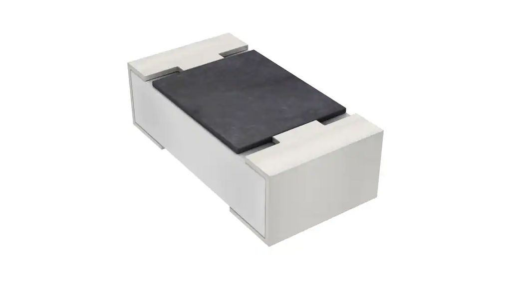
Würth Elektronik supply SMT inductors such as the MAPI and MAIA series. MAPI power inductors offer high current capability and handles high transient current spikes. They are magnetically shielded, offering low acoustic noise, low leakage flux noise, and high rated current thanks to their magnetic iron alloy.
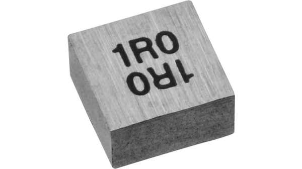
The WE-MAIA is one of the smallest metal alloy power inductors on the market. Its efficiency is remarkable, and the 4020HT series now comes in new sizes and extended temperature versions with AEC-Q200 Grade 0 approval for operation temperatures ranging from -55 to +150 degrees Celsius. Discover more in the catalog of the series.
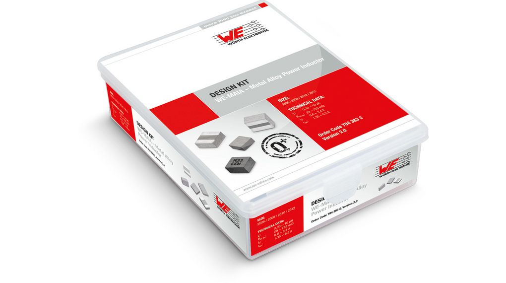
For circuit prototyping purposes, the Würth Elektronik MAIA metal alloy power inductor design kit offers a convenient evaluation resource. It covers the full range of inductors in the series; a data sheet for the kit is available here.
KEMET offers a comprehensive range of capacitors, including surface-mount MLCCs, and larger, higher voltage axial and radial leaded devices. The EIA classifies these MLCCs as “temperature stable” and Class II materials. Class II capacitors are fixed ceramic dielectric capacitors that are suitable for bypass and decoupling applications as well as frequency discriminating circuits where capacitance Q and stability are not crucial.
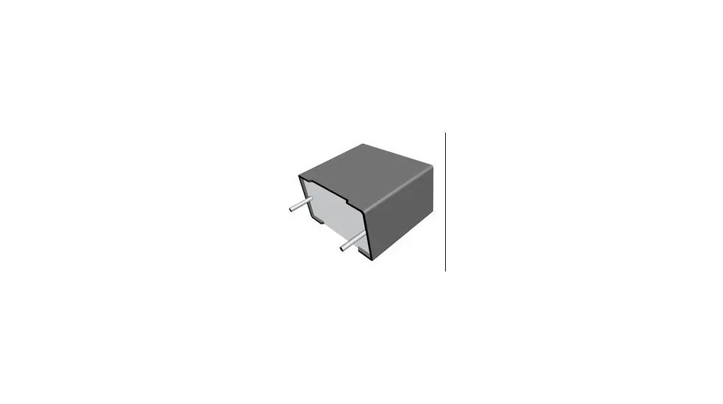
Other series is the C4AU offering a high voltage, automotive-qualified capacitor suitable for use in harsh electrical environments, particularly for DC link applications. The C4AU Series is a metallized film capacitor made of polypropylene that has a high capacitance density and high contact reliability. The series is an excellent example of product innovation, where the techniques of metalised film capacitors have enabled product miniaturisation. An informative white paper about the C4AU development is available here.
The Distrelec website showcases the broad KEMET range of capacitors suitable for various applications.
Component miniaturisation in the industrial domain
End-product manufacturers are keen to take advantage of the continual size reduction of electronic components. The industrial sector, in particular, has seen the degree of automation used increase significantly over the last decade. Industrial efficiency improvement initiatives, such as Industry 4.0 and the industrial internet of things (IIoT), are responsible for the increasing deployment of electronics-based sensors, control equipment, and AI machine learning systems. This increase in automation equipment is set against the backdrop of available factory space at a premium, driving demand for compact, energy-efficient, and leading-edge component technologies.
The drive to component miniaturisation is not limited to electronic components. Manufacturers of automation equipment and sub-assemblies have also been innovating. Advances in 3D printing, material technology research and a deeper understanding of finite element analysis in mechanical design contribute to weight, size, and cost reductions.
Industrial component miniaturisation showcase
Ultrasonic sensors are employed in various object detection tasks such as safety cages and products on a conveyor belt. An example of a compact ultrasonic sensor is the Baumer U300 series. It uses an ultrasonic emitter operating at 310 kHz to provide a detection range up to 1 m. The U300 series measures 12.9 mm x 32.2 mm x 23 mm and takes up considerably less space than the previous generation of detection sensors. Connection to the host controller is achieved using an 8-pin M12 round industrial connector and is IP67 rated. Baumer offers a comprehensive line-up of sensors designed specifically for industrial applications.
Another industrial sensor manufacturer is Wachendorff. A product example is the LMSCA32 ultra compact length measurement system. This system measures the length of materials, wood, metal, fabrics etc., during a manufacturing process using a 200 mm measurement wheel rotation.
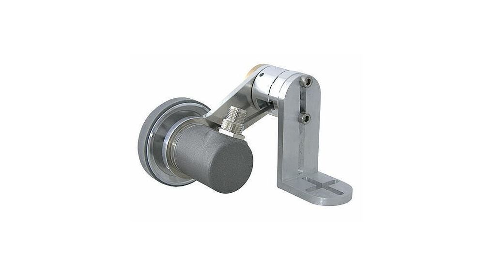
An ultra-compact system with new spring-loaded arm maintains wheel contact with the measured material, and the rotary encoder sends out pulses as the wheel rotates. The resolution frequency of the pulses is configurable from 200 pulses per revolution (ppr) to 16,000 ppr.
The benefits of component miniaturisation
The ongoing trend of component miniaturisation enables designers and manufacturers to incorporate more advanced features into their end-products while also reducing their footprint. Whether designing an IIoT sensor or an industrial programmable logic controller, you can realise space savings within the product enclosure. Miniaturisation allows for the design of more stylish and space-efficient products. It also opens up the opportunity to increase the features and functionality of new products without increasing their dimensions.


