Additive manufacturing opens up a whole new world for electronics and goes beyond its former purpose.
Electronics surround us all, from laptops and smartphones to digital cameras and wearables. Yet, not everyone knows how exactly they operate inside and what their true potential is. Most electronics, to work properly, rely on electronic components, such as sensors, connectors, antennas and printed circuit boards (PCBs). Now, they can be 3D printed.
With the solutions from Voltera, you can discover how additive manufacturing brings new ways to create components using different materials, things that were not possible to achieve with traditional electronics. Thanks to the materials’ compatibility, they can be embedded into the world.
Using additive manufacturing for PCB prototyping
3D printing is popular in many industrial applications as one of the most common methods for creating prototypes. However, additive manufacturing is much more than just prototyping. By 3D printing electronics it is possible to make various types of boards that can be programmed and connected to prototypes. Printed electronics and flexible hybrid electronics (FHE) are two growing additive manufacturing industries that allow prototyping and product iteration on a desktop versus outsourcing PCB production to a third-party supplier.
3D print PCBs offer greater design flexibility than traditional circuit boards. Designers are now able to experiment with a wide range of layers, geometries, and shapes to create forms that were not possible to make in any other way. Research, innovation and product improvement are fluid processes, so the ability to design and test concepts in the creative moment is one of the key benefits of using additive manufacturing for your PCB prototyping.
There are plenty of benefits and advanced solutions that win over traditional prototyping methods.
Benefits of 3D print PCBs
- Greater design flexibility, e.g. creating materials that imitate skin
- Less waste products (greener electronics)
- Reduction in production cost
- Quick design to production time
- Adding new functionalities to electronics
- Material compatibility and better customisation
Materials for new electronic products
Additive electronics opens up the possibility for people to start producing entirely new items. The material compatibility allows designers to add new functionalities into electronics that can be embedded in the world.
Using 3D printing allows people to print different materials, like carbon, semiconductor materials, conductors or even resistive materials for heaters. Besides, those new types of materials can be printed in specific form factors, and also on different types of materials. For example, with 3D printing it is possible to design a rubber/stretchable material that has mechanical properties of a skin, or wearables that are integrated into the user’s body. Making things like these weren’t possible with traditional prototyping.
“It is not about making things cheaper or faster, or even making them potentially greener, it is about adding a new functionality to the electronics. From electronics that are boards in boxes inside our phones to electronics that are ambiguous, embedded in the world that we live in – into the structure of buildings we occupy, clothing we are wearing or even our skin”
– Matt Ewertowski, Project Manager of the NOVA
Additive manufacturing brings more freedom to the electronics design, as the traditional manufacturing process is often precisely defined. This 3D method can encourage people to alter the production process so that it may be completed internally, giving designers and mechanical engineers much more creative freedom.
Choosing the ideal PCB substrate material
Whether it will be a completely new innovation or just a customisation of existing items, the materials, or rather substrates play a key role (substrate is the technical word in materials science for the substance or material that the designer intends to apply a feature or design on).
Traditional PCB Substrates
In traditional manufacturing, the most common PCB substrates are:
- FR4 – the most popular type of PCB material is a glass-reinforced epoxy laminate that is 1.60 mm thick and flame retardant (FR). It has a maximum temperature threshold of 120 to 130°C for the glass transition temperature and is made of eight layers of fibreglass material. It absorbs almost no water, has good strength to weight ratios, and is frequently used as an electrical insulator. The main thing to keep in mind with this material is that it requires drilling through-holes for the project (i.e., need a two-sided board). For that, an FR1 board might be required instead of an FR4 board because the latter might be harmful due to the fibreglass dust it produces. However, with proper masking and ventilation, this is definitely something possible to work around.
- FR1 – similar to the FR4, these boards are composed of paper and phenolic resin rather than fibreglass, making them less expensive and simpler to construct. It does, however, affect their ability to withstand heat; for example, when heated during the reflow process or with thermally cured conductive inks, they may scorch or deform. The other issue to keep in mind is that vias for double-sided boards cannot be produced using conventional PCB manufacturing paradigms because plating through holes on FR1 is not possible. However, with the PCB Printer V-One, it is possible to drill attachment to create holes in FR1 boards, and you can use rivets to create functionally plated through-holes for double-sided boards.
Flexible Printed Electronics Substrates
Examples of flexible printed electronics substrates:
- Polyimide Films (AKA Kapton) – ideal for applications that require to withstand harsh conditions like radiation, vibration, or extreme temperatures. Also, it will work whenever saving space is important, like smart watches, smartphones, laptops and airpods. Hence it is perfect for uses like wearable electronics or microelectronics, where size and weight affect how a product will ultimately look and feel. It can be shaped, punched, or metalized, and because it can be laminated on both sides, bonded to other materials like metals or other films, or even filled, it can practically be made to fit any need.
- Polyethylene terephthalate (PET) – a strong, transparent, and light plastic, frequently used in food and drink packaging (e.g. 2L Coke bottle). PET is an inert and entirely recyclable material. It should be taken into account given the toxicity and damage caused by the conventional copper etching procedure for PCBs. PET is much less expensive than polyimide, but there is a downside; the maximum temperature ranges from 140 to 160°C and it is less thermally and dimensionally stable.
Stretchable Printed Electronic Substrates
Stretchable materials, like we mentioned earlier, bring a completely new view on additive manufacturing, allowing designers to create things that weren’t possible before. For example tissue engineering and prosthetics which are popular applications of additive manufacturing in healthcare.
- Thermoplastic polyurethane (TPU) is a subclass of polyurethane plastics that exhibits a number of desirable characteristics for use in flexible electronics, including transparency, flexibility, grease and oil resistance, and abrasion resistance. Due to its stretchability, it is also a great material for wearable electronics and the textile sector. TPU powders are also utilised in 3D inkjet printing and laser sintering procedures.
- Polydimethylsiloxane (PDMS) is a substrate that is especially beneficial for items that must stretch. Yet, due to its use in stretchy applications, along with its exceptional thermal stability, transparency, and biological compatibility, it is not something that is easily available for purchase. Instead, many researchers will cast their own PDMS. The learning curve for casting PDMS is somewhat steep, but once you get the hang of it, it’s really not that difficult.
Modified Paper Printed Electronic Substrates
The last type, a modified paper printed electronic substrate, is basically about printing on paper (which seems like the most common thing when thinking about printing), but it is not such a sturdy material, so it might absorb conductive ink (more about inks below). There are a variety of coated and processed papers being developed to address this issue, enabling applications, including smart packaging, wearable technology, and textiles.
PCBs with conductive inks
Selecting an ink requires making a number of crucial choices, all of which are based on what you want your device to be able to achieve. After you are aware of the requirements for your application, you can choose an ink.
A conductive ink can be:
- Printed — adding pattern to your surface.
- Processed — in order for conductive ink to become a conducting material, it must be processed, usually by heating it.
- Conductive — a type of functional ink, or inks with uses other than those related to aesthetics or structural requirements.They are creating a route for electrons to go from point A to B.
What are conductive inks made of?
- Filler — this is the conductive substance—typically metal particles—that will give your ink its electrical capabilities. The most frequently utilised filler is silver, thanks to its superior stability and easy to use features. The second one is copper which is frequently used to make traditional PCBs using subtractive techniques like etching.
- Vehicle — all other substances that suspend your particles, including binders, dispersants, solvents, and additives. This process allows the ink to flow and dry, and gives it structural ability and flexibility.
To find out more about conductive inks, go to Voltera’s blog that gives a comprehensive overview on inks used for PCBs.
Printing process
After successfully choosing the right material and ink, finally you can consider the printing process of the conductive ink onto the selected material. Which printing technology works the best for you? It depends on the project’s size and scope, the learning environment, the materials needed, and whether the goal is purely exploratory study or the development of a finished product.
Luckily, whether it is a usual design or something that pushes the boundaries, with components from Voltera, you can do everything at your workbench. Voltera offers tools and materials, providing help without the need of material science, for example by providing its customers with printable inks, that speed up the manufacturing process without thinking about how to print the idea. Also, in their offer there is a ready PCB printer that enables users to quickly print PCBs to desktops. The V-One can print traces of conductive ink, drill through holes and vias, precisely dispense solder paste and reflow components with a built-in heater.
Watch the video below to discover the V-One functionalities or scroll to the bottom to buy a V-One PCB printer now.
Have a look at the technologies below and choose the correct ink for the printing process you intend to use.
InkJet
InkJet might be the most commonly known method and you are correct if you assume that this sounds like the technology used by your home office printer. The fact that this technology is digital is one of the key benefits of adopting it for printed electronics and quick prototyping in general. Iteration time is significantly decreased because any modifications to your design can be printed immediately without the need for extra tooling. The technology relies on ejecting tiny droplets from hundreds of tiny nozzles on a print head in quick succession to form a pattern on the substrate.
Advantages:
- High-resolution printing
- Low material cost
- Design printed using a digital file
Disadvantages:
- Higher resistance
- Susceptible to breaking, or incomplete circuit printing
- Susceptible to improper storage conditions
- Difficult to solder components onto
- High printer system costs
Note: Inkjet printing requires low viscous inks, with low metallic content – while this helps with resolution, in addition to the final product having poor electrical performance – the materials are not representative with industry standards and hence not scalable.
Better option is the direct write technology because it allows to dispense the same conductive pastes used in screen printing, roll2roll, etc. which are used in large scale manufacturing of flex PCBs. Hence prototypes are much more representative and scalable.
Screen Printing
This is an ancient technology that became popular as utilities for everything. From printing graphic t-shirts to making additive electronics. Screen printing is one of the most well-known production processes because of its versatility, which is a result of technological advancements in the field. Conductive ink is printed onto a substrate via screen printing for additive electronics using a finely woven mesh. When the wiper or squeegee passes over the screen, the holes in the mesh are blocked with a masking substance (or emulsion) to stop ink from being deposited onto the substrate there.
Advantages:
- Compatible with a wide range of materials
- Layers with a typical thickness ranging between 10-35 µm
- Lower resistance
- Versatile
- Low initial investment
- Consistency and saving time
- Scalable
Disadvantages:
- Low resolution (feature size of around 25-50µm — but that’s pushing the limits of screen printing technology. In practice, you’re looking at 200-300µm from a commercial printer)
- High tooling and safety equipment costs
- Difficult materials experimentation
- Material waste
Flexography
Flexography, also referred to as “flexo printing” is essentially a modernised letterpress that can print on nearly any substrate, including plastic, cellophane, paper, metal, and more. To transfer the ink through tiny holes to the substrate, it mounts a flexible printing plate on spinning cylinders that spin quickly. The list of benefits and drawbacks for this one is essentially the same as that for gravure because the two technologies are so close.
Advantages:
- Great for high volume printing
- Substrate flexibility
Disadvantages:
- Challenging as this technology isn’t as straightforward or well adopted in the industry of printed electronics
Gravure
Gravure is the process where the image is created in the depressions or recesses on the surface of the printing plate, in contrast to relief printing where the image is lifted from the surface of the printing plate. After the grooves on the plate have been etched to create the picture, you fill the recesses with ink, set the plate down on the substrate, and the ink is deposited onto the substrate from the recesses.
Advantages:
- Great for high volume printing
Disadvantages:
- Expensive (this method relies on the laser etching of your design onto a metal plate, iterating becomes increasingly expensive)
- Substrate limitations
- Need a low viscosity conductive ink
Aerosol
The conductive ink used in this printing technique is atomised into a dense mist with droplets that are 1 to 5 micrometres in size, which is then focused into a narrow stream of droplets by a sheath gas. The outcome is a high-velocity particle stream that may print between 2 and 5 mm from the surface of your substrate.
Advantages:
- High resolution patterns
- Can print on complicated shapes, like 3D objects
Disadvantages:
- Low volume, low throughput
- Steep learning curve
- Cost-prohibitive due to increased materials costs
Direct Write
Direct-write technique, also known as 3D printing via direct extrusion, applies force and dispenses conductive ink from a cartridge using pneumatics, pistons, or screws. A conductive ink in the 1-200 kcP (Pa·s) range is required for this technology to function correctly, while advancements in the technology will expand these limits. Usually, something a little thicker works better. Also, you should choose a filler material that will provide you with the greatest alternatives. For tasks that need higher resistive materials, carbon or silver are more frequently used as a result.
Advantages:
- Extremely adaptive and flexible, fitting any circumstance or use case you can think of (you can “print anything on everything,” so long as you have the right equipment (a design file, a printer, ink, and substrate).
- Only applies ink to the areas you choose
- Gives you access to the z-axis
- Easy to change materials
- Less expensive
- Easy adoption
- Good resolution
- Iterating is easy
Disadvantages:
- Scalability – not possible to do high-volume printing (instead, you should choose a process that is easier to scale up, such as screen printing).
To find out more about which ink would be the best for your project and learn about conductive inks and direct-write technology, read this ultimate Voltera’s guide or contact Voltera directly. They will assist you in choosing an ink and help to produce something ambiguous. As Matt Ewertowski, the Project Manager of the NOVA, says ‘it is all about making materials more accessible.’
Recommended products
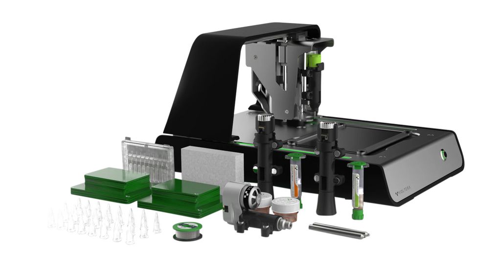
PCB Printer, V-ONE, Voltera
The V-One can precisely distribute solder paste, drill through-holes and vias, print conductive ink traces, and reflow components using an integrated heater. The Voltera V-One is an all-in-one board fabrication solution that keeps your development cycle short and all of your IP in-house.
Features:
- Desktop, multi-functional circuit board printer.
- Easy to use with simple software.
- All-in-one solution for board fabrication.
- It can drill through-holes and vias, precisely dispense solder paste, and reflow components with an integrated heater in addition to printing conductive ink traces.
- Rapid iteration as you can export the Gerber file the same day after finishing your design.
Find out more specifications in the datasheet here.